
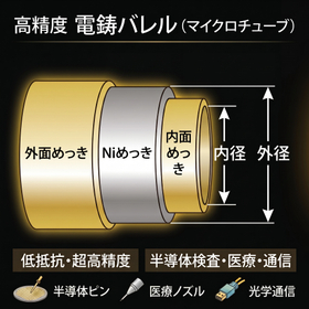
【Semiconductor and Wafer Inspection】Ultra-high precision electroforming barrel (microtube)
Achieving ultra-high precision that is difficult with cutting processes. By reducing resistance through inner and outer surface plating, we solve the challenges of extending the lifespan of semiconductor testing probes and medical components.
■ Do you have any of these challenges? - Struggling with the short lifespan of probe pins in semiconductor and wafer inspections - Feeling limited in precision for ultra-small sizes in cutting and seamless processing - Looking for precision components for image inspection and high-precision medical parts ■ "Electroformed Barrel (Microtube)" will solve this Our unique electroforming technology enables the production of ultra-high precision electroformed barrels that are difficult to achieve with conventional processing. Utilizing electrochemical reactions, we can manufacture with high precision on both inner and outer diameters. Additionally, by applying plating to both the inner and outer surfaces, we achieve low resistance. ■ Benefits of Implementation & Main Applications 【Semiconductors】 Leads to longer lifespan of probe pins and high-precision inspections due to low resistance. 【Medical & Industrial】 Fine nozzles for dispensers 【Communication】 Can be used as micro connectors for optical communication. *Customization is available according to your requirements, including inner diameter, outer diameter, total length, and hardness. For more details, please check the PDF by clicking "Download Catalog" below, or feel free to contact us.
- Company:ニデックアドバンステクノロジー 本社、東京営業所、名古屋営業所
- Price:Other
